
Bootstrap Protocol
Pavona discrete top-level designs with nonvolatile memory support a bootstrap protocol, which allows a host to load software to nonvolatile memory. The bootstrap protocol is designed to conform to well-known standards and be driven by commonly available equipment. The reference ROM implementation in the Pavona code uses the SPI interface for performing bootstrap operations. Support for bootstrapping over other HWIPs such as I2C and USB may be added in the future.
The bootstrap protocol is intended for the following use-cases:
- Loading manufacturing firmware during the Final Test (FT) provisioning stage.
- Firmware loading for development and debug of chips in the
DEVlifecycle state. - Disaster recovery situations in-field, such as a wiped nonvolatile storage.
The bootstrap protocol is not intended for:
- Performing routine firmware updates.
- Transferring ownership of the chip at any boot stage.
The SPI bootstrap protocol is designed to operate using the typical SPI flash EEPROM command set and driven by commonly available SPI flash programmers (e.g. the Dediprog SF100). It makes discovery and diagnostic information available via standard SPI flash mechanisms. It is also designed to have deterministic timing bounds on long-running operations (such as ERASE and PROGRAM) so unidirectional programmers can be used, such as the Automated Test Equipment (ATE) used during provisioning.
Activation
The bootstrap mechanism is activated by asserting the SW_STRAP_BOOTSTRAP on the correct strapping pins.
The bootstrap mechanism in the reference Pavona ROM does not require authentication to enter bootstrap mode, nor does it perform any validation on the loaded data contents. The ROM validates the contents of the nonvolatile memory during its secure boot process and will not permit execution of unauthorized code.
It is the host’s reponsibility to prevent unauthorized (remote) access to the bootstrap mechanism. While an attacker cannot use the bootstrap protocol to run unauthorized code on the chip, they can perform a denial-of-service attack by erasing the chip and then aborting the bootstrap protocol. Recovery from this attack requires initiating another bootstrap with a valid payload.
Note: The manufacturer has the option to disable bootstrapping by writing to the CREATOR_SW_CFG_ROM_BOOTSTRAP_DIS OTP bit.
Operation
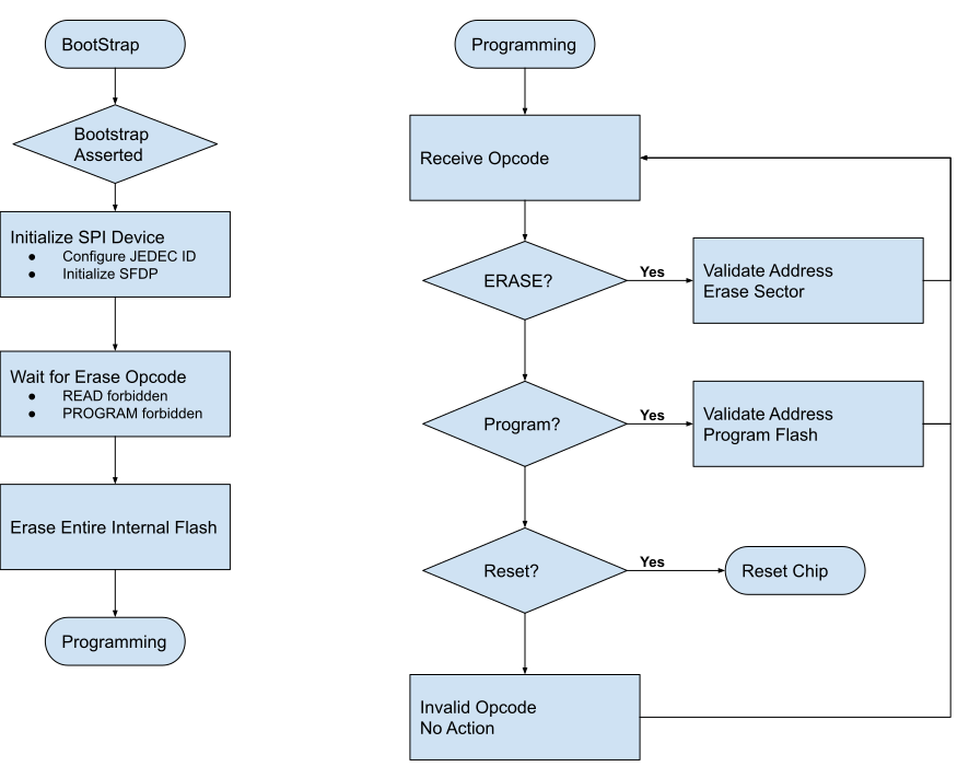
The ROM bootstrap protocol consists of the following steps.
Note: the following description does not include a description of complete opcode sequences for a given operation (e.g. an ERASE normally requires WRITE_ENABLE, ERASE and then a READ_STATUS until the BUSY bit clears).
- If the
CREATOR_SW_CFG_ROM_BOOTSTRAP_DISOTP bit is unset, check forSW_STRAP_BOOTSTRAPon the correct straps. - If
SW_STRAP_BOOTSTRAPwas sent, the ROM enters bootstrap mode. - Upon entering bootstrap mode, initialize EEPROM discovery mechanisms, such as the JEDEC ID and Serial Flash Discovery Parameters (SFDP) Table.
- Wait for an
ERASEorSECTOR_ERASEopcode; all other operations are ignored.READs will return a static buffer of 0xFF.PROGRAMoperations will do nothing.
- Upon receiving an
ERASEorSECTOR_ERASEopcode, bootstrap erases the internal nonvolatile data partitions and then enter a generic SPI flash opcode dispatch loop. The erase operation will not affect any of the info partitions. - Within the generic opcode dispatch loop:
- An
ERASEopcode will erase all nonvolatile data partitions. - A
SECTOR_ERASEopcode will validate the supplied address and erase the target sector. - A
PAGE_PROGRAMopcode will validate the supplied address and program the target page. - A
RESETopcode will exit the dispatch loop and reset the chip.
- An
Public API
// Determine whether or not bootstrap mode has been requested by
// examining the strapping pins configuration.
bool bootstrap_mode_check(void);

// Enter into bootstrap mode and perform the update protocol.
// - Initialize the SPI Device
// - Configure SPI JEDEC ID and SFDP tables.
// - Listen and act on SPI transactions
rom_error_t bootstrap_mode_enter(void);
Test Plan
The bootstrap module will use unit tests to validate the proper operation at the module boundaries.
The bootstrap module will also have functional tests which use verilator to simulate the bootstrap flows via the SPI device interface. These tests will check for valid operation of the bootstrap flows and will check that the properties of each bootstrap phase perform their intended functions and correctly abort when the protocol sequence is violated.
Because the bootstrap module implements the real-world programming interface, testing flows must be developed which verify bootstrap functionality on FPGA devices paired with real programmer devices such as the Dediprog SF100. Any difficulties encountered with the physical devices should result in enhanced tests performed in the unit tests or function tests.
Note
On rare occasions, there will be a problem with the exiting bootstrap protocol, which usually presents as corrupted SHA checksums (usually in the form of a dropped bit). These can normally be worked around by ignoring the checksums.
There are also reports of occasional synchronization issues with the full-duplex protocol.